- 您现在的位置:买卖IC网 > Sheet目录1997 > ICS843021AGLFT (IDT, Integrated Device Technology Inc)IC CLK GENERATOR LVPECL 8-TSSOP
ICS843021AG REVISION D OCTOBER 12, 2010
6
2010 Integrated Device Technology, Inc.
ICS843021 Data Sheet
FEMTOCLOCK CRYSTAL-TO-3.3V LVPECL CLOCK GENERATOR
Applications Information
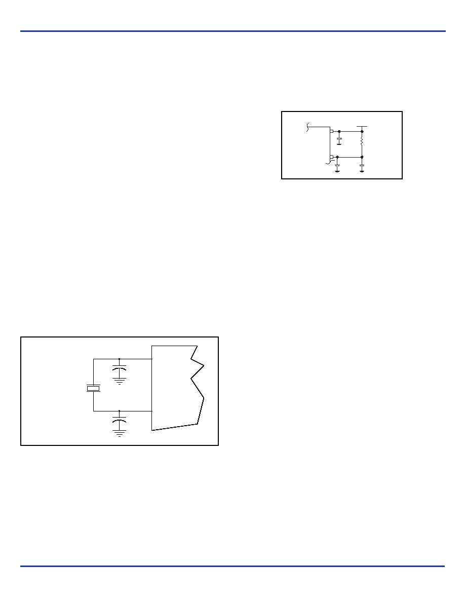
Power Supply Filtering Technique
As in any high speed analog circuitry, the power supply pins are
vulnerable to random noise. To achieve optimum jitter performance,
power supply isolation is required. The ICS843021 provides separate
power supplies to isolate any high switching noise from the outputs
to the internal PLL. VCC and VCCA should be individually connected
to the power supply plane through vias, and 0.01F bypass
capacitors should be used for each pin. Figure 1 illustrates this for a
generic VCC pin and also shows that VCCA requires that an additional
10
resistor along with a 10F bypass capacitor be connected to the
VCCA pin.
Figure 1. Power Supply Filtering
Crystal Input Interface
The ICS843021 has been characterized with 18pF parallel resonant
crystals. The capacitor values, C1 and C2, shown in Figure 2 below
were determined using a 25MHz, 18pF parallel resonant crystal and
were chosen to minimize the ppm error. The optimum C1 and C2
values can be slightly adjusted for different board layouts.
Figure 2. Crystal Input Interface
VCC
VCCA
3.3V
10
10F
.01F
XTAL_IN
XTAL_OUT
X1
18pF Parallel Crystal
C1
33pF
C2
27pF
发布紧急采购,3分钟左右您将得到回复。
相关PDF资料
ICS843022AGLF
IC CLK GENERATOR LVPECL 8-TSSOP
ICS843023AGLF
IC CLK GENERATOR LVPECL 8-TSSOP
ICS843031AG-01LF
IC CLK GENERATOR LVPECL 8-TSSOP
ICS843081AGI-01LF
IC CLK MULTIPLIER LVPECL 8-TSSOP
ICS8430AYI-61LF
IC SYNTHESIZER LVPECL 32-LQFP
ICS8430S07AKILF
IC CLK GENERATOR PLL 32VFQFN
ICS8430S10BYI-02LF
IC CLK GENERATOR PLL 48TQFP
ICS84314AY-02LFT
IC SYNTHESIZER 700MHZ 32-LQFP
相关代理商/技术参数
ICS843021AGT
制造商:ICS 制造商全称:ICS 功能描述:FEMTOCLOCKS-TM CRYSTAL-TO- 3.3V LVPECL CLOCK GENERATOR
ICS843021I-01
制造商:ICS 制造商全称:ICS 功能描述:FEMTOCLOCKS-TM CRYSTAL-TO-3.3V, 2.5V 125MHZ LVPECL CLOCK GENERATOR
ICS843022
制造商:ICS 制造商全称:ICS 功能描述:FEMTOCLOCKS-TM CRYSTAL-TO- 3.3V LVPECL CLOCK GENERATOR
ICS843022AG
制造商:INT_DEV_TECH 功能描述:
ICS843022AGI-48LF
功能描述:IC CLK SYNTHESIZER LVPECL 8TSSOP RoHS:是 类别:集成电路 (IC) >> 时钟/计时 - 时钟发生器,PLL,频率合成器 系列:HiPerClockS™, FemtoClock™ 标准包装:1,000 系列:- 类型:时钟/频率合成器,扇出分配 PLL:- 输入:- 输出:- 电路数:- 比率 - 输入:输出:- 差分 - 输入:输出:- 频率 - 最大:- 除法器/乘法器:- 电源电压:- 工作温度:- 安装类型:表面贴装 封装/外壳:56-VFQFN 裸露焊盘 供应商设备封装:56-VFQFP-EP(8x8) 包装:带卷 (TR) 其它名称:844S012AKI-01LFT
ICS843022AGI-48LFT
功能描述:IC CLK SYNTHESIZER LVPECL 8TSSOP RoHS:是 类别:集成电路 (IC) >> 时钟/计时 - 时钟发生器,PLL,频率合成器 系列:HiPerClockS™, FemtoClock™ 标准包装:1,000 系列:- 类型:时钟/频率合成器,扇出分配 PLL:- 输入:- 输出:- 电路数:- 比率 - 输入:输出:- 差分 - 输入:输出:- 频率 - 最大:- 除法器/乘法器:- 电源电压:- 工作温度:- 安装类型:表面贴装 封装/外壳:56-VFQFN 裸露焊盘 供应商设备封装:56-VFQFP-EP(8x8) 包装:带卷 (TR) 其它名称:844S012AKI-01LFT
ICS843022AGLF
功能描述:IC CLK GENERATOR LVPECL 8-TSSOP RoHS:是 类别:集成电路 (IC) >> 时钟/计时 - 时钟发生器,PLL,频率合成器 系列:HiPerClockS™, FemtoClock™ 标准包装:1,000 系列:- 类型:时钟/频率合成器,扇出分配 PLL:- 输入:- 输出:- 电路数:- 比率 - 输入:输出:- 差分 - 输入:输出:- 频率 - 最大:- 除法器/乘法器:- 电源电压:- 工作温度:- 安装类型:表面贴装 封装/外壳:56-VFQFN 裸露焊盘 供应商设备封装:56-VFQFP-EP(8x8) 包装:带卷 (TR) 其它名称:844S012AKI-01LFT
ICS843022AGLFT
功能描述:IC CLK GENERATOR LVPECL 8-TSSOP RoHS:是 类别:集成电路 (IC) >> 时钟/计时 - 时钟发生器,PLL,频率合成器 系列:HiPerClockS™, FemtoClock™ 标准包装:1,000 系列:- 类型:时钟/频率合成器,扇出分配 PLL:- 输入:- 输出:- 电路数:- 比率 - 输入:输出:- 差分 - 输入:输出:- 频率 - 最大:- 除法器/乘法器:- 电源电压:- 工作温度:- 安装类型:表面贴装 封装/外壳:56-VFQFN 裸露焊盘 供应商设备封装:56-VFQFP-EP(8x8) 包装:带卷 (TR) 其它名称:844S012AKI-01LFT